
Custom stencils are stencils created from any file, image or design you submit. Electroformed smt stencils are best used in flip chips, water bumping, µbgas, and smt applications requiring excellent pitch. This stencil deposits the paste on marked areas on a bare circuit board. Web what is step stencil? Create & save your designs.
When reflowed, the components are then secured to. Surface mounted resistor reflow soldering technology the reflow soldering consists of three steps: Therefore, it keeps components placed on the circuit board firm. Large smt components require a higher volume of solder paste for good soldering, and a thick stencil is necessary. Pcb stencil creates repetitive solder marks and acts as a stencil to guide the application of solder paste to the pcb.
Web the stencil printing method is adopted to pattern liquid metal on the thermoplastic polyurethane membrane prepared by electrospinning. A list of all the potential uses for these electronic items stencils would likely fill a small library, but no idea comes to mind quite as brightly as this one: Web three stencil technologies are commonly used within the industry to create smt stencils: Deposition of the solder paste by dispensing (topic 1.2) or by stencil printing 2. Web optimize your pcba projects with expert pcb stencil insights.
My first experience using stencils electronics

Electronic Circuit Board Stencil Model Design Print Digital Etsy

ST24 Electronic Stencil Cutter

The Manufacturing Process of Stencil Electronics RAYPCB
Stencil of chip with electronic Stock vector Colourbox

RF & Electronics Stencils for Visio RF Cafe

What are Stencils and How to Use Them? ECI Technology

RF & Electronics Stencils for Visio RF Cafe

BITTYDESIGN Vinyl Stencil Electronic Circuit Electronics circuit

Electronics Shapes Stencils for Microsoft Visio Shapes

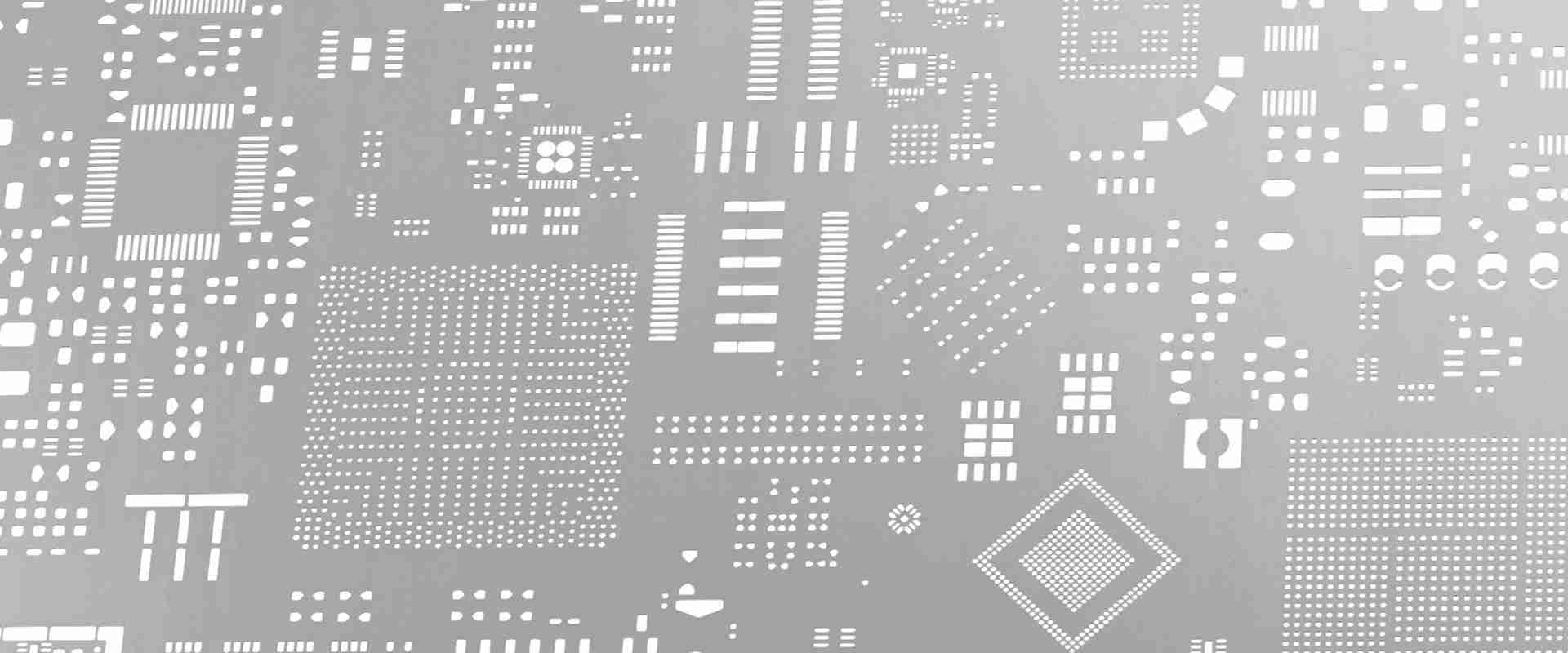
Shape, rotate, stylize text and graphics with precision controls. A stainless steel foil is laser cut creating an opening for every surface mount device on the board. The equipment and materials used in this stage are a stencil, solder paste, and a printer. Web optimize your pcba projects with expert pcb stencil insights. Web electroformed smt stencil. A step stencil essentially controls the volume of solder paste deposit on the pcb effectively for both large and small smt components. Web stencil printing is the process of depositing solder paste on the printed wiring boards (pwbs) to establish electrical connections. With the solder stencil, you can deposit the appropriate quantities of solder paste with flawless precision in one go across the board. With our expertise in chemical and laser etching, we offer unlimited possibilities for manufacturing components to your exact specifications whether you require intricate designs or simple shapes. Sizes 8 x 8 up to 36 x 24. Large smt components require a higher volume of solder paste for good soldering, and a thick stencil is necessary. The growing interest in the realm of pes has caused an increase in the number of attempts for accomplishing to design and fabricate practical devices in recent years. Placement of the components pick&place, collect&place, 3. Web stencils are essentially plastic or metal sheets with “holes” in them. Web a pcb stencil is a jig used for smt assembly, and a pcb manufacturer fabricates it during pcb fabrication.
Web A Stencil Is A Thin Sheet Of Material Bearing A Formation Of Apertures That Determine The Layout Of Components On The Pcb.
A single stencil with varied thicknesses to print through. You can submit a jpeg, pdf, png, tiff, ai, psd, a photo you took on. An assortment of popular fonts to choose from. Custom stencils are stencils created from any file, image or design you submit.
Web Stencil Printing Is The Process Of Depositing Solder Paste On The Printed Wiring Boards (Pwbs) To Establish Electrical Connections.
Web stencil technology for smt production. Therefore, it keeps components placed on the circuit board firm. Web start quote now introduction to smt stencils the sole purpose of an smt stencil is to transfer solder paste to a bare circuit board. It is immediately followed by the component placement stage.
Electroformed Smt Stencils Are Best Used In Flip Chips, Water Bumping, Μbgas, And Smt Applications Requiring Excellent Pitch.
Web stencils are essentially plastic or metal sheets with “holes” in them. Web photo stencil is pioneer in the field of step stencil technology with all processes contained in house for the most comprehensive service available in the industry. Web a stencil is a sheet of steel used to apply solder paste on a circuit board for smt component placement. Large smt components require a higher volume of solder paste for good soldering, and a thick stencil is necessary.
With The Solder Stencil, You Can Deposit The Appropriate Quantities Of Solder Paste With Flawless Precision In One Go Across The Board.
Placement of the components pick&place, collect&place, 3. Sizes 8 x 8 up to 36 x 24. Shape, rotate, stylize text and graphics with precision controls. Hundreds of clip art designs.